
To understand Electrical Impedance let us first take a quick look at some PCB Basics.
PCB BASICS
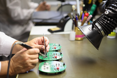
PCB stands for Printed Circuit Boards, which is essentially a board with components that are connected by traces or wires. Before the invention of PCBs, electrical circuits were built using wires instead of the more efficient and cleaner ‘copper’ traces used in these modern Circuit Boards.
The PCB is one of the most important components in this modern world of ours, you just don’t see it. But if you were to crack open any modern gadget you have today, you can almost be certain that it contains a type of PCB.
What is a PCB made of?
In most designs, the PCB is made of four layers: A Silkscreen, Soldermask, Copper, and a Substrate.
- The Silkscreen is the uppermost layer where you will add the symbols and markings for your PCB to allow for better understanding of the board. The markings are important because even if you designed the board, after a couple of months it will be difficult to trace your components easily without the visual aid.
- The Soldermask provides the color of the Circuit Board and is the insulator that prevents the copper traces from getting shorted by other conductors. This layer makes it easier to find the right places to solder within the circuit board.
- The Copper layer is an important part of the PCB, and there can be multiple layers of copper in it. This is where the electric current passes, acting as the lifeline of your PCB. The thickness of the copper is indicative of the amount of power the board can handle.
- The Substrate layer constitutes the majority of the overall thickness of the board. A number of different materials can be used as the substrate layer. The most common practice is to use fiberglass. You can also have a flexible substrate for PCBs that are designed to withstand high-temperatures called Kapton. Cheaper boards use epoxy and phenolics, which may significantly bring the quality of the PCB down.
Jumping into Impedance
What is it? Electrical impedance is the effective opposition of the materials used in a circuit (e.g. copper wires and traces) to an Alternating Current (AC). For Direct Currents impedance is equal to resistance.
Before the advent of better computers and other electrical gadgets the electrical impedance of a given circuit used to be negligible. But with higher and higher frequencies, the circuit boards will behave like transmission lines and due to impedance, the electricity travelling through the traces could reflect back and forth. If you are unsure on how to make proper calculations for your PCB design you could bring in outside allegro layout services to help you with a design that can accommodate the impedance factor accurately.
How about Controlled Impedance
A good PCB design would need to have electrical impedance taken into account. This means that all traces within a given board should have uniformed impedance (or essentially controlled impedance).
If you brought in allegro layout services, then you should discuss with the designer the correct or ideal width of the trace, its thickness, the length of the space between the signal trace and signal return path, and the dielectric constant of the material that surrounds the trace.
Controlled impedance is a vital aspect that must be tackled if you are to create an efficiently designed PCB. Contact us today for more information!